


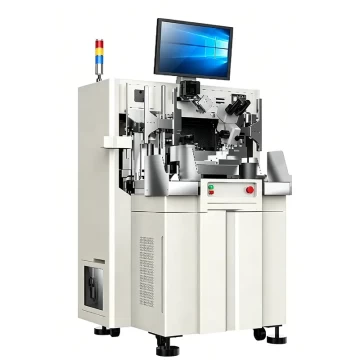
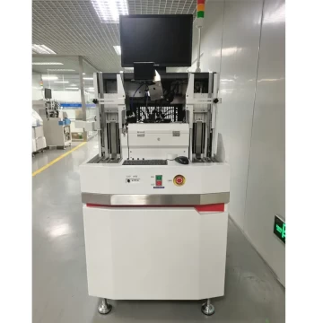


Fully Automatic Compound Semiconductor Cleaving Line System BO-9070
Supplied and Integrated by: Jiangsu Himalaya Semiconductor Co., Ltd.
Technically Reviewed by: Dr. Jian Li · Senior Process Engineer, Semiconductor Equipment Division
Introduction
In compound semiconductor chip manufacturing, cleaving, scribing, and breaking are decisive processes that directly affect chip yield, facet quality, and long-term device reliability. For high-end applications such as optical devices, laser chips, and optical communication chips, the Fully Automatic Compound Cleaving Line System BO-9070 delivers an integrated cassette-to-cleaved-chip workflow — combining cassette loading, compound cleaving and scribing, fully automatic film mounting, and fully automatic breaking in a single automated line.
The system is supplied and integrated by Jiangsu Himalaya Semiconductor Co., Ltd., a Suzhou-based specialist in the high-level integration and international trade of advanced semiconductor manufacturing equipment.
About the Supplier
Jiangsu Himalaya Semiconductor Co., Ltd. has been active in the semiconductor equipment industry since 2019, serving 200+ customers and suppliers across 30+ countries. The company specializes in the high-level integration and international trade of advanced manufacturing equipment, providing cost-effective, high-performance solutions with risk-managed global transactions.
Its equipment portfolio covers:
-
Bonding & Marking — die bonders, wire bonding, laser marking for IC wafer traceability
-
Laser Processing — laser grooving and cutting for glass, ceramics, and wafer packaging; internal modification for Si/SiC and LT/LN wafers; laser annealing for Si/SiC substrates
-
Dicing & Dispensing — automatic dicing saw machines; automatic silicone dispensing equipment
-
Customized Industrial Solutions — TGV (Through Glass Via) equipment in manual, semi-automatic, and fully automatic configurations; coating and plating systems; environmental and resource management solutions
This breadth allows Jiangsu Himalaya Semiconductor to position the BO-9070 as part of an integrated production line rather than a standalone tool.
Applications: Covering Major Chip Manufacturing Segments
The BO-9070 is designed for major chip manufacturing applications, with particular focus on:
-
Optical Devices — chips with stringent cleaved facet quality requirements
-
Laser Chips — GaAs, InP, and GaN compound semiconductor laser bars and chips
-
Optical Communication Chips — compound chip cleaving, scribing, and breaking
The system is compatible with wafers, bars, GaN bars, and CELLs, supporting both high-mix low-volume and large-scale production environments.
Key Features
Independent Light Source Brightness Setting
Light source brightness can be configured independently according to product function and position. This design effectively addresses product-to-product variation — a practical advantage when switching between GaAs, InP, and GaN products with differing reflectivity and surface characteristics.
Four Core Functions Integrated
-
Cassette Loading — supports cassettes with 25 iron rings
-
Compound Cleaving and Scribing — high-precision cleaving and scribing
-
Fully Automatic Film Mounting — automatic film mounting after scribing
-
Fully Automatic Breaking — fully automatic breaking operation
From cassette loading through breaking completion, the entire process is automated, reducing manual handling of thin, brittle compound substrates.
Industrial Vision
An industrial vision system efficiently recognizes wafer outlines and Notch positions, providing a reliable visual reference for precise positioning across different wafer sizes and types.
Multi-Product Compatibility
Compatible with fully automatic operation for wafers, bars, GaN bars, and CELLs — a single system covering multiple product forms.
SEMI Standard with SECS-GEM Communication
Compliant with SEMI standards and supporting SECS-GEM communication, enabling seamless integration with factory automation systems and MES-driven environments.
Key Specifications
| Parameter | Details |
|---|---|
| Substrate Materials | GaAs, InP, GaN, SiC, Si |
| Processing Sizes | 4 / 6 / 8 inches |
| Bar Chips | Bar 4.5 mm × 30 mm; single chip 0.10 mm × 4.5 mm |
| X-Y Stage Travel | 160 mm × 160 mm |
| Positioning Accuracy | Repeat positioning accuracy: ±2 μm; positioning accuracy: ±2 μm |
| Transfer System | Load port, robot, aligner |
Processing Results: High-Precision Positioning Ensures Cleaving Quality
With repeat positioning accuracy and positioning accuracy of ±2 μm, combined with industrial vision for wafer outline and Notch recognition, the BO-9070 maintains stable processing quality throughout compound cleaving, scribing, and breaking.
For a single chip dimension of 0.10 mm × 4.5 mm, a ±2 μm positioning error represents approximately 2% of the 0.10 mm die width — acceptable for most compound semiconductor cleaving applications. Fully automatic film mounting and breaking further reduce human-induced effects on cleaved facets, supporting improved chip yield and consistency.
Why Source Through Jiangsu Himalaya Semiconductor
-
Global sourcing reach — 30+ countries, 200+ qualified customers and suppliers
-
Cost-performance filtering — deep industry expertise applied to global option screening
-
Risk-managed transactions — supplier-friendly payment collection and comprehensive risk avoidance
-
Portfolio breadth — one partner across bonding, laser processing, dicing, dispensing, TGV, and coating
Technical Review
Reviewed by: Dr. Jian Li · Senior Process Engineer, Semiconductor Equipment Division · 15+ years in die bonding, micro-assembly, and advanced packaging
Review Scope
This technical review evaluates the BO-9070 Fully Automatic Compound Cleaving Line System as presented for compound semiconductor cleaving, scribing, film mounting, and breaking applications. The assessment covers process capability, positioning accuracy relevance, automation architecture, and fit with mainstream compound semiconductor production environments.
1. Process Positioning and Relevance
Compound semiconductor cleaving is a facet-critical process. In laser diode and optical communication chip manufacturing, the cleaved facet directly determines optical output quality, threshold current and efficiency, and long-term reliability. Unlike dicing, cleaving relies on crystallographic plane separation, making it highly sensitive to scribe depth and alignment, substrate crystal orientation, and mechanical breaking force uniformity.
The BO-9070's integration of scribing and breaking in one automated line is the correct architectural choice. Separating these steps across multiple tools introduces handling risk, alignment drift, and yield loss — particularly for thin GaAs and InP wafers.
Assessment: Process architecture is appropriate for the target applications.
2. Positioning Accuracy — Practical Interpretation
The stated ±2 μm repeat positioning accuracy and ±2 μm positioning accuracy on a 160 mm × 160 mm stage is a meaningful specification for this class of equipment.
| Process Requirement | Relevance of ±2 μm |
|---|---|
| Scribe line placement on bar | Directly determines facet quality |
| Notch/outline alignment | Ensures crystal-orientation-correct cleaving |
| Multi-bar processing consistency | Reduces bar-to-bar variation |
| CELL-level handling | Supports small die geometries |
Assessment: Specification is credible and appropriate; process qualification recommended for critical laser applications.
3. Automation Architecture
The BO-9070's four integrated functions represent a full cassette-to-cleaved-chip workflow. Technical strengths include reduced manual handling (critical for thin, brittle compound substrates), in-line film mounting that minimizes contamination and handling damage between scribe and break, and SEMI-standard SECS-GEM communication for automated fab and MES integration.
Considerations for evaluation include verifying film mounting quality (bubble-free, uniform tension) empirically, characterizing breaking force control and repeatability across bar lengths, and measuring cassette-to-cassette throughput with actual product.
Assessment: Automation scope is well-matched to volume compound semiconductor production.
4. Vision System and Product Flexibility
The industrial vision system for wafer outline and Notch recognition addresses a known pain point in compound semiconductor manufacturing: inconsistent wafer edge quality and orientation marking. Independent light source brightness control — configurable by product function and position — is a practical feature, since lighting is a common source of vision failure when switching between GaAs, InP, and GaN products.
Assessment: Vision and lighting design show awareness of real production variability.
5. Compatibility Review
The BO-9070 supports GaAs, InP, GaN, SiC, and Si substrates at 4/6/8-inch sizes, with compatibility for wafers, bars, GaN bars, and CELLs. This is a broad but coherent compatibility profile that aligns with the wider equipment portfolio offered by Jiangsu Himalaya Semiconductor.
6. Limitations and Verification Recommendations
| Item | Status | Recommendation |
|---|---|---|
| Throughput (UPH) | Not stated | Request empirical data |
| Breaking force repeatability | Not stated | Request characterization report |
| Film mounting defect rate | Not stated | Request sample inspection |
| Scribe depth control method | Not detailed | Request technical documentation |
| Uptime / MTBF | Not stated | Request field reliability data |
| Process qualification data | Not provided | Request customer references |
These are not deficiencies in the equipment — they are gaps in the published information. Any serious procurement evaluation should request this data directly.
7. Reviewer Conclusion
The BO-9070 presents a technically sound architecture for compound semiconductor cleaving: integrated scribing, film mounting, and breaking, with positioning accuracy appropriate for the target die geometries and SEMI-compliant automation for modern fabs.
Strengths:
-
Correct process integration for facet-critical applications
-
±2 μm positioning suitable for 0.10 mm-class die
-
Broad substrate and product compatibility
-
Industrial vision with product-adaptive lighting
-
SECS-GEM ready
Recommended next steps for evaluation:
-
Request throughput and reliability data
-
Request process qualification samples on your substrate
-
Validate film mounting quality
-
Confirm SECS-GEM integration with your MES
-
Review service and spare parts support model
For compound semiconductor manufacturers evaluating cleaving automation — particularly those in laser, optical device, and optical communication segments — the DC-CP8060 warrants inclusion in a shortlist, subject to empirical process validation.
Frequently Asked Questions (FAQ)
Q1: What substrate materials does the BO-9070 support?
A: GaAs, InP, GaN, SiC, and Si.
Q2: What wafer sizes does the system process?
A: 4/6/8 inches, plus bar chips (bar 4.5 mm × 30 mm; single chip 0.10 mm × 4.5 mm).
Q3: What is the positioning accuracy?
A: Repeat positioning accuracy ±2 μm; positioning accuracy ±2 μm.
Q4: Does it support factory automation communication?
A: Yes — it complies with SEMI standards and supports SECS-GEM communication.
Q5: What are the main functions of the system?
A: Cassette loading (25 iron rings), compound cleaving and scribing, fully automatic film mounting, and fully automatic breaking.
Q6: Can it handle different product types?
A: Yes — wafers, bars, GaN bars, and CELLs, with independent light source brightness setting to address product variation.
Q7: How do I request a quote or consultation?
A: Contact Jiangsu Himalaya Semiconductor Co., Ltd. by phone or WhatsApp at +86 15995822759, email seaman@himalayasemi.com, or visit the address below.
Contact Us
| Field | Details |
|---|---|
| Company | Jiangsu Himalaya Semiconductor Co., Ltd. |
| Phone | +86 15995822759 |
| +86 15995822759 | |
| seaman@himalayasemi.com | |
| Address | Room 4234, Building 11, No. 1258 Jinfeng South Road, Mudu Town, Wuzhong District, Suzhou City |
| Postal Code | 215101 |