


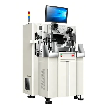
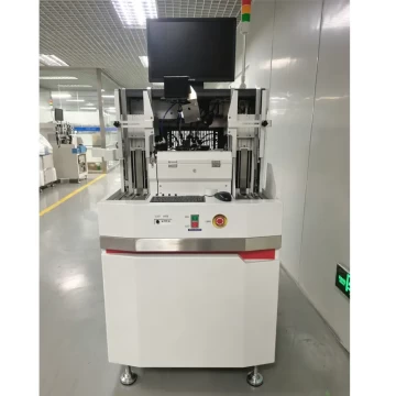


High-Precision Fiber Alignment System: Maximizing Optical Coupling Efficiency
What Is a Fiber Alignment System?
A fiber alignment system is an integrated hardware and software solution engineered to position optical elements—including single-mode fibers, laser diodes, VCSELs, and Photonic Integrated Circuits (PICs)—with extreme positional accuracy. The system dynamically aligns components across up to 6 degrees of freedom (XYZ + θₓ, θᵧ, θ_z) to achieve peak optical power transmission while minimizing insertion loss.
Why Precision Alignment Is Critical
-
Accumulative Signal Degradation: Optical networks feature numerous junction interfaces. Misalignments of less than 1% compound into severe signal loss across the optical path.
-
Capital Cost Reduction: Optimizing coupling efficiency lowers the laser drive power requirements, eliminating the need for expensive inline optical amplifiers or repeaters.
-
Thermal & Operational Reliability: Precise positional alignment ensures long-term power stability in harsh environment enclosures and hermetically sealed modules.
System Architecture & Hardware Specifications
| Component | Architecture & Mechanism | Key Technical Specifications |
|---|---|---|
| Nanopositioning Stage | Closed-loop piezo-actuated or servo-motor driven (6-Axis) | • Resolution: 1 nm • Repeatability: ±10 nm |
| Optical Power Monitor | In-line InGaAs photodetector array | • Dynamic Range: -70 dBm to +10 dBm • Wavelengths: 1260–1650 nm |
| Vision System | High-magnification CCD/CMOS with IR backlight | • Field of View: 50 µm – 5 mm • Sub-pixel Accuracy: <50 nm |
| Light Source | Tunable laser diode array | • Spectral Bands: C-band (1530–1565 nm), O-band (1260–1360 nm) |
| Control Software | Real-time feedback loop running gradient descent / hill-climbing algorithms | • Active Cycle Time: <5 seconds • Automation: Batch process support |
Alignment Methodologies: Active vs. Passive
1. Active Fiber Alignment
Active alignment uses active optical feedback during positioning to maximize power coupling.
-
Accuracy: <0.1 µm (Sub-micron)
-
Coupling Efficiency: >90% (Single-Mode Fiber to Laser Diode)
-
Optimal For: High-performance laser diodes, edge-emitting lasers, PIC-to-fiber attachment, and high-density transceivers.
2. Passive Fiber Alignment
Passive alignment relies on mechanical registration features, such as silicon V-grooves, etched fiducials, or machine vision without active light monitoring.
-
Accuracy: ±0.5 µm to ±2.0 µm
-
Cycle Time: Sub-second positioning per channel
-
Optimal For: Mass production of silicon photonics wafer-level packaging where process speed overrides ultra-low loss requirements.
Step-by-Step Fiber Alignment Process
1. Vision-Guided Coarse Alignment
High-magnification machine vision cameras capture edge features and fiducials, moving the nanopositioning stage within a 5 µm envelope of the optical aperture.
2. First Light Detection
The active software executes a rapid spiral or raster scan pattern to detect initial optical power above the power monitor's threshold (typically > -50 dBm).
3. Peak Power Search Optimization
Real-time feedback algorithms (such as hill-climbing, dichotomy, or AI-driven gradient optimization) adjust the 6-axis stage to locate the absolute maximum optical coupling peak.
4. Position Lock & Verification
The system locks piezo positions via closed-loop feedback, confirming power stability across a brief vibration/drift observation window.
5. Fixation & Packaging
The aligned assembly is permanently fixed in place using UV-curable optical adhesives, laser welding, or thermosonic wire/flip-chip bonding.
Industry Benchmarks & Metrics
| Performance Metric | Typical Standard | High-Volume Telecom Benchmark |
|---|---|---|
| Positioning Accuracy | <50 nm | <100 nm (for >95% coupling) |
| Positional Repeatability | ±10 nm | ±20 nm (post thermal cycling) |
| Coupling Efficiency | >90% (SMF) | >80% (400G / 800G optical transceivers) |
| Total Cycle Time | <10 seconds | <30 seconds (full automated packaging) |
Key Applications
-
Silicon Photonics: Edge coupler and grating coupler alignment for optical interconnects.
-
Co-Packaged Optics (CPO): Multi-channel fiber ribbon to photonic chip packaging.
-
LiDAR & Quantum Computing: Laser diode array coupling to nanophotonic wave-guides and single-photon detectors.
Author & Publisher Information
Author: Dr. Jian Li, Senior Process Engineer, Semiconductor Equipment Division
15+ years experience in die bonding, micro-assembly, and power device packaging.
Publisher: Jiangsu Himalaya Semiconductor Co., Ltd.
Established in 2019, specializing in advanced back-end semiconductor equipment export, micro-assembly solutions, and precision wafer dicing equipment.
Locations
-
Headquarters & R&D:
Room 4234, Building 11, No. 1258 Jinfeng South Road, Mudu Town, Wuzhong District, Suzhou City, Jiangsu Province, China -
Sales Office:
No. 58, Keji 3rd Road, High-Tech Zone, Yanta District, Xi'an, China