


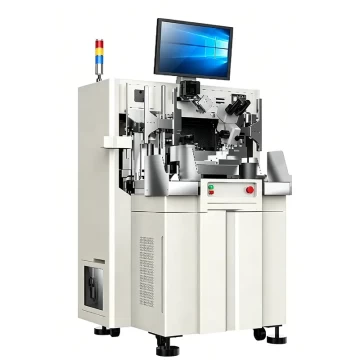
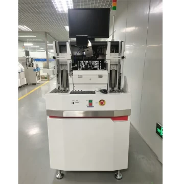


Laser Stealth Dicing Systems: Complete Procurement & Technical Guide for GaN, SiC, and Sapphire Wafers
Introduction: Why Laser Stealth Dicing Is Transforming Compound Semiconductor Manufacturing
As demand for GaN-on-SiC, GaN-on-sapphire, SiC, and sapphire-based devices surges across power electronics, RF communications, and optoelectronics, manufacturers face a critical challenge: how to dice brittle, hard, and expensive compound semiconductor wafers without compromising die quality or yield.
Laser stealth dicing (LSD) has emerged as the answer. Unlike conventional blade dicing or abrasive methods, stealth dicing uses a focused laser beam to create internal modified zones within the wafer material, enabling clean separation with minimal chipping, no kerf loss, and no water or debris contamination.
This article provides a comprehensive technical procurement framework for a wafer dicing system using laser stealth dicing — covering equipment specifications, module-by-module requirements, and key considerations for R&D and low-volume production environments.
What Is Laser Stealth Dicing?
Laser stealth dicing is a non-ablative, dry dicing process that focuses a pulsed laser beam inside the wafer substrate. The laser induces localized structural modification (often called "stealth zones" or "modified layers") along intended dicing streets. Subsequent expansion of the adhesive carrier tape causes controlled crack propagation through the wafer thickness, separating individual dies.
Key advantages for compound semiconductors:
-
No chipping or micro-cracks on die edges (critical for GaN/SiC devices)
-
No water or coolant required — compatible with sensitive passivation layers
-
High throughput — cutting speeds up to 300 mm/s
-
Material versatility — GaN on SiC, GaN on sapphire, SiC, sapphire
-
Thin wafer capability — 100 µm to 550 µm thickness
-
Minimal kerf loss — maximizing die per wafer
Equipment Purpose: A Complete Dicing Workflow
A laser stealth dicing system for compound semiconductor wafers must integrate multiple process steps into a single, automated platform:
-
Wafer mounting onto adhesive carrier tape
-
Laser stealth dicing of wafers into individual dies
-
Wafer expansion on the adhesive carrier after dicing
-
UV irradiation of UV-curable adhesive tape
Each step requires precise control, material compatibility, and automation for reproducible results.
Core Technical Specifications: What to Require
1. Wafer Compatibility
| Parameter | Requirement |
|---|---|
| Wafer diameters | 100 mm, 150 mm, 200 mm |
| Materials | GaN on SiC, GaN on sapphire, SiC, sapphire |
| Thickness range | 100–550 µm |
| Surface layers | Residual GaN-based materials and/or SiN-type passivation up to 15 µm above substrate on dicing street |
| Die dimensions (L × W) | 0.5 × 0.5 mm to 30 × 30 mm |
2. Positioning and Motion Accuracy
| Parameter | Requirement |
|---|---|
| X-axis positioning accuracy | ≤ 3 µm |
| Y-axis positioning accuracy | ≤ 3 µm |
| Z-axis travel | 20 mm |
| Z-axis positioning accuracy | 1 µm (note: some systems offer 1.5 µm — verify against requirement) |
| θ-axis resolution | 0.1 µm |
| Dynamic focus control | Required |
3. Cutting Performance
| Parameter | Requirement |
|---|---|
| Cutting speed | Up to 300 mm/s (inclusive) |
| Wafer dicing modes | Manual and automatic |
4. Automation and Vision
| Parameter | Requirement |
|---|---|
| Automatic manipulator | Required for handling wafers on adhesive carrier |
| Automatic wafer loading/unloading | Required |
| Machine vision system | Required for automatic recognition of dies and dicing streets |
| Software | Creation and storage of technological process algorithms |
| Control system | PC- and SW-based, keyboard, mouse, touch panel interface |
Module-by-Module Requirements
Module 1: Wafer Mounting onto Adhesive Carrier (Tape)
This module mounts wafers onto thermal or UV-curable tape. If not integrated, it must be available as a standalone system.
| Parameter | Requirement |
|---|---|
| Wafer diameter | 100, 150, 200 mm |
| Tape type | Thermal, UV-curable |
| Tape roll width | Up to 300 mm |
| ESD protection | Required |
| Working chuck | Vacuum clamp, no contact with planar side of wafer |
| Chuck heating | 65 ± 1 °C, digital indicator |
| Temperature setting increment | 1 °C |
| Wafer frame positioning | Centering mechanism |
| Longitudinal cutter | Required for trimming tape on roll |
| Circular cutter | Required for trimming tape along frame |
| Adhesion uniformity | No air bubbles, wrinkles, or delamination |
| Control system | Controller with display |
| Protective layer winding roller | Required |
| Wafer thickness | 100–550 µm |
| Processed materials | GaN on SiC, GaN on sapphire, SiC, sapphire |
| Loading/unloading | Manual or automatic |
| Vacuum system | Required for clamping and air removal |
Module 2: Wafer Breaking (Cleaving) After Laser Processing
After laser stealth dicing, the wafer must be separated into individual dies. This module applies controlled force to break the wafer along laser-modified streets.
| Parameter | Requirement |
|---|---|
| Wafer diameter | 100, 150, 200 mm |
| Wafer thickness | 100–550 µm |
| Die size compatibility | 0.5 × 0.5 mm to 30 × 30 mm |
| Control system | PC- and SW-based, keyboard, mouse, or touch-screen controller |
| Recipe storage | Required |
| Processed materials | GaN on SiC, GaN on sapphire, SiC, sapphire |
| Breaking force | Adjustable with feedback loop and program-controlled settings; must fully break SiC/sapphire |
| Die quality after breaking | Chipping ≤ 15 µm on front and back; no cracks; no incompletely broken dies |
| Operating mode | Manual or automatic |
| Y-axis linear accuracy | ± 5 µm |
| Y-axis positioning repeatability | ± 1 µm |
| Z-axis linear accuracy (lift) | ± 5 µm |
| Z-axis positioning repeatability (lift) | ± 1 µm |
Module 3: Wafer Expanding on Adhesive Carrier After Dicing
Expansion separates dies on the tape after laser processing and breaking.
| Parameter | Requirement |
|---|---|
| Wafer diameter | 100, 150, 200 mm |
| Drive type | Servo |
| Plunger travel / increment | 50 mm / 1 mm |
| Expanding speed | 40–50 mm/s |
| Chuck heating / increment | Up to 55 °C / 1 °C |
| Die size compatibility | 0.5 × 0.5 mm to 30 × 30 mm |
| Control system | Controller with touch screen |
Module 4: UV Tape Irradiation
UV irradiation reduces tape adhesion for easy die pickup.
| Parameter | Requirement |
|---|---|
| Maximum UV intensity | 400 mW/cm² |
| Wavelength | 365 ± 3 nm |
| Processing area | 240 × 240 mm |
| Wafer diameters | 100, 150, 200 mm |
| Irradiation time / increment | 1–100 s / 1 s |
| Radiation power control / increment | Required / 1% |
| Minimum loading area | 370 × 370 mm |
| Cooling type | Air cooling |
| Control system | Digital display indicator and control elements |
Consumables and Accessories: What Must Be Included
A complete procurement package must include:
| Item | Quantity |
|---|---|
| Metal frames/formers for wafers (type DTF 2-8-1) | 30 pcs |
| Expander rings for wafer expanding | 50 pcs |
| UV tape for wafer dicing (width 285 ± 5 mm) | 100 meters |
| Standard tape for wafer dicing (width 285 ± 5 mm) | 100 meters |
| Spare parts, tools, and accessories (ZIP) kit | Sufficient for warranty period |
| Software copy on electronic media | 1 |
| Operation and maintenance documentation (Russian, hard copy + electronic) | Complete set |
| Equipment passport | 1 |
Compatibility note: Metal frames must be compatible with the dicing system without additional adaptation.
Warranty, Support, and Training Requirements
| Requirement | Specification |
|---|---|
| Warranty period | At least 12 months from Acceptance Test Report signing |
| Warranty coverage | All units, mechanisms, electronic components, software |
| Installation, setup, commissioning | Performed by Supplier |
| Process startup and acceptance tests | Per specification agreed with Supplier |
| Technical support | Required |
| Personnel training | Russian language, ≥ 2 specialists, ≥ 5 working days |
| Equipment condition | Brand new (not refurbished) |
| Intended use | R&D and low-volume production |
| Preliminary acceptance | At manufacturer's/supplier's facility |
| Final acceptance | On Customer's territory after installation, setup, commissioning |
Compliance Verification: Manufacturer's Technical Specification
All equipment technical characteristics must be verified by the manufacturer's technical specification (in Russian or English) for the proposed equipment model. This ensures that the supplied system meets every requirement of the technical assignment.
Frequently Asked Questions (FAQ)
What is laser stealth dicing?
Laser stealth dicing is a dry, non-ablative wafer dicing method that focuses a pulsed laser inside the wafer to create modified zones along dicing streets. The wafer is then expanded on adhesive tape, causing controlled cracking and die separation.
Why is stealth dicing preferred for GaN, SiC, and sapphire?
These materials are hard, brittle, and expensive. Stealth dicing minimizes chipping, avoids water contamination, and enables thin wafer processing with high yield.
What wafer thicknesses can be processed?
The system must handle 100 µm to 550 µm thickness, including residual GaN-based materials and/or SiN-type passivation up to 15 µm above the substrate on the dicing street.
What die sizes are supported?
From 0.5 × 0.5 mm to 30 × 30 mm.
What is the maximum cutting speed?
Up to 300 mm/s, inclusive.
What positioning accuracy is required?
X-axis and Y-axis: ≤ 3 µm. Z-axis: 1 µm (some systems offer 1.5 µm — verify against requirement).
What tape types are compatible?
Thermal and UV-curable tapes, with roll width up to 300 mm.
What UV wavelength is required for tape irradiation?
365 ± 3 nm, with maximum intensity of 400 mW/cm².
What is the warranty period?
At least 12 months from the date of signing the Acceptance Test Report.
Is training included?
Yes — training in Russian for at least 2 specialists, with duration not less than 5 working days.
Is the equipment new or refurbished?
The equipment must be brand new (not refurbished).
What is the intended use?
R&D activities and low-volume production.
Key Takeaways for Procurement Professionals
-
Material versatility is critical — Ensure the system handles GaN on SiC, GaN on sapphire, SiC, and sapphire.
-
Thickness range matters — 100–550 µm with accommodation for passivation layers up to 15 µm.
-
Positioning accuracy drives yield — X/Y ≤ 3 µm, Z = 1 µm.
-
Automation reduces operator error — Automatic manipulator, loading/unloading, and machine vision are required.
-
Module integration or standalone flexibility — Mounting, breaking, expanding, and UV irradiation must be available as integrated or standalone systems.
-
Consumables must be included — Frames, expander rings, UV tape, standard tape, ZIP kit, software, and documentation.
-
Training and support are non-negotiable — Russian-language training for ≥ 2 specialists, ≥ 5 days.
-
Compliance verification — Manufacturer's technical specification must confirm all requirements.
-
Warranty and acceptance — 12-month minimum warranty; preliminary acceptance at supplier facility, final acceptance on Customer territory.
-
Brand new equipment only — No refurbished systems.
Conclusion
Procuring a laser stealth dicing system for GaN, SiC, and sapphire wafers requires careful attention to material compatibility, positioning accuracy, module integration, and consumable completeness. This technical guide provides a comprehensive framework for specifying, evaluating, and accepting such equipment for R&D and low-volume production environments.
By following these requirements — from wafer mounting through UV irradiation — procurement teams can ensure they select a system that delivers high die quality, minimal chipping, and reliable performance for advanced compound semiconductor manufacturing.